

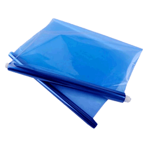
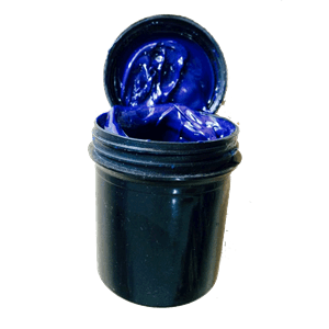
It is known that the circuit patterns need to be moved to circuit boards from CAD files, a series of processes and materials are required. During the exposure and development processing, the uses a kind of cleanable chemical protective films to transfer the circuit patterns to CCL, they are usually divided into dry film and wet film (resist).
Both of dry film and wet film are photosensitive materials that react chemically under specific wavelengths of light.
The dry film and the wet film are similar in usage, Take dry film as an example for simple introduction here.
The most common production process is to put the dry film-attached CCL under the film with the circuit pattern and expose/develop it in the UV machine. The dry film uncovered by circuit pattern gets hardened, meanwhile, the covered dry film can be removed. Next, the bare copper wire is tinned and then coated with etch resist, and the hardened dry film and the underlying copper are removed in the etching process, finally, you get the desired circuit traces.
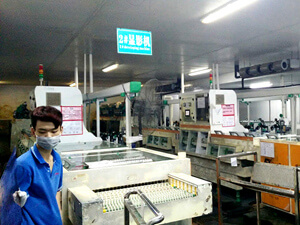
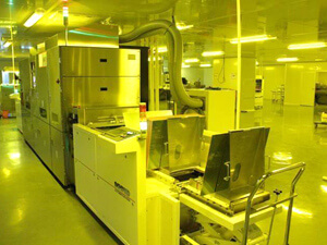
transfers circuit patterns to CCLs by a series of automatic machines, probably you cannot see the processing inside the machines. But for DIY PCB making, the dry film is also required, based on the same principle, the excellent video below may clarify the processing for you.