

PCB panel is generally necessary for , the purpose of the designing of PCB panel is nothing more than the following two factors:
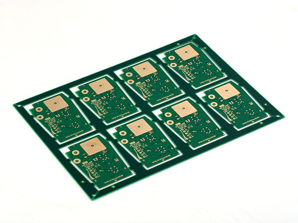
The most common PCB panel is usually consist of two or more identical circuit boards into a large circuit board. A rectangle PCB board is good for manufacturing, so the PCB panel design is frequently even number, such as 2 in 1, 4 in 1, 8 in 1, etc. . It is also possible to form a large PCB panel with circuit boards of different shapes, but it is rare, because it complicates the production processing, which results in that different-sub PCB panel design requires extra fee in many PCB shops.
There are other PCB panel designs in actual , such as mirror-board, which means that the same number of boards are on the same side of an PCB panel. This is usually used for fewer parts mounting, such as mobile phone boards, of which the advantage is the lines can be fully utilized, but the disadvantage is that there are restrictions on use, and it may cause uneven heating of parts.
Basically, when designing PCB panel, the following 3 factors should be considered. In fact, no matter how you produce or design, you can’t walk around the consideration of money. Therefore, all the factors should be converted into the cost-effective consideration to find out the suitable PCB panel.
For rapid mass production and low cost, general circuit board manufacturers will order the raw materials in the standard dimensions, such as 16.16"x16.16", 18"x24", 20.32"x20.32", etc., what should be done is to use up the area of a standard CCL as possible, that is, to choose a suitable standard dimension, try to pack the most pieces in a PCB panel to achieve the highest utilization rate.
Because the price of a circuit board generally depends on the total area, the more the PCBs can fit in one PCB panel, the cheaper the price. Of course it is a simplified concept, the price of a circuit board also has to consider layer-count, drilling-number, whether there is , etc.
An PCB panel with the length of 150mm is used as an example. The printing time of a solder paste takes about 35 to 40 seconds. If only a 2 in 1 PCB panel is used, in a short-term SMT line, the time allocated to each post-set machine is about 10 to 26 seconds, which is obviously lower than the solder paste printing time, means that all of the placement machines will wait for solder paste printing completion. This will cause idle SMT machines and reduce production capacity.
If you change 2 in 1 PCB panel into to 4 in 1, the efficiency will increase immediately, as shown.

After PCB panelization, there will be a very serious problem, that is, the expansion rate of the board will increase. As the PCB panel gets bigger and bigger, the dimensional tolerance between the pieces will drag down subsequent SMT processing, reduce yield, especially for the SMDs that are smaller than 0402.
Because the opening of stencil is fixed, if the size difference between the pieces is too large, the solder paste printing will be shifted as a whole. Once the solder paste is shifted, the tombstone, short circuit, empty soldering ... the problems will follow.
X-out is additional consideration for PCB panel design, which means there are several bad pieces in an PCB panel. The more the pieces in one PCB panel, the higher the probability of X-out. If X-out is unacceptable, the cost of production raises, which also led to your cost raise.
So as mentioned, the factors should be converted into cost-effective considerations then you will find out the panelization method for your projects. And the results may be slightly different for different PCB factories.